Designing a high-speed PCB involve lots of critical factors that go beyond standard PCB design rules. With industries like communications, aerospace, and IoT rapidly evolving, more engineers are diving into high-speed PCB design. However, these designs require additional considerations that may not be familiar to many designers. In this article, we’ll break down the most important aspects of high-speed PCB design and share key insights into materials, stackups, and impedance control.
Choosing the Right High-Speed PCB Material
The material selection plays a vital role in high-speed PCB performance. While FR-4 epoxy laminate is the industry standard, its dielectric properties may not be ideal for signals operating in the hundreds of MHz to GHz range. For better signal integrity at high frequencies, Rogers materials like RO4003C and RO4350B are widely preferred due to their superior electrical characteristics.
High-Speed PCB Stackups & Layering
High-speed design PCBs often fall into the High-Density Interconnect (HDI) category, requiring a well-planned multilayer stackup to support high-speed signals. Custom stackups are essential to achieving optimal performance for signal integrity and reduce signal loss. If your design includes microvias, blind vias, or buried vias, ensure HDI manufacturing capabilities can accommodate those requirements.
Impedance Control for High-Speed Signals
Maintaining signal integrity in high-speed designs often requires controlled impedance to ensure proper transmission of differential pairs and matched impedance traces. Team with high expertise can perform impedance control calculations and simulations to develop a stackup that meets your specifications, preventing signal loss and distortion.
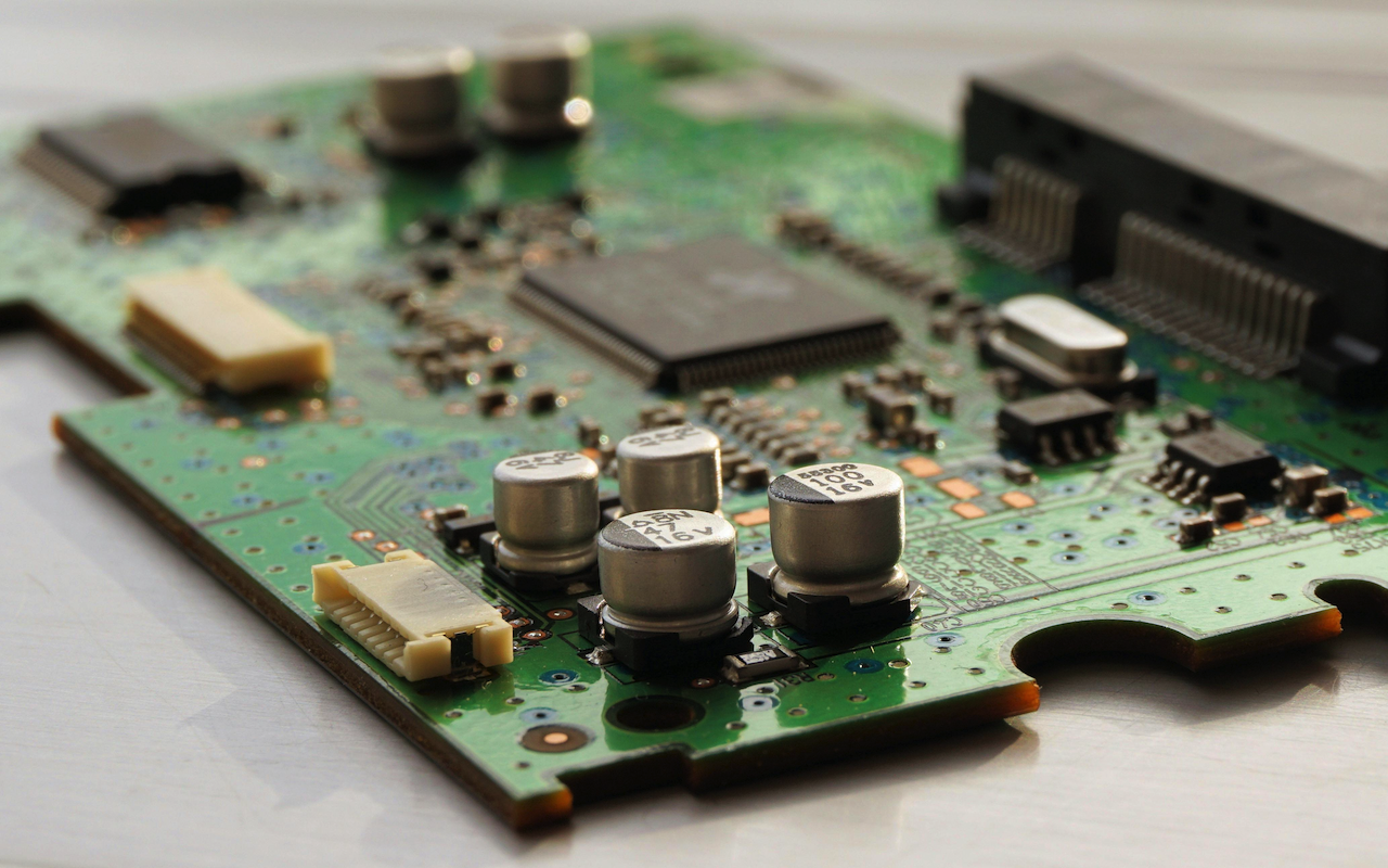
PCB Assembly Considerations
Once the design phase is complete, the PCB assembly process becomes crucial. High-speed PCBs often require precise assembly techniques to ensure that the components are placed accurately and that the solder joints are reliable. Factors such as component placement, solder paste application, and reflow soldering profiles must be carefully controlled to avoid introducing noise or signal integrity issues. Collaborating with an experienced PCB assembly provider can help mitigate these risks and ensure that the final product performs as intended.
Conclusion
Designing and building a high-speed PCB demands a comprehensive approach that accounts for advanced materials, precision layering, controlled impedance, and meticulous assembly processes. Each decision—from material selection to stackup configuration and assembly techniques—can significantly impact the board’s performance, especially in applications where speed and signal integrity are paramount. The above art just a few of the many factors to consider when designing a high-speed PCB.
Share this post
Leave a comment
All comments are moderated. Spammy and bot submitted comments are deleted. Please submit the comments that are helpful to others, and we'll approve your comments. A comment that includes outbound link will only be approved if the content is relevant to the topic, and has some value to our readers.
Comments (0)
No comment